Introduction
The upgraded role of cubesats, fueled by technological advances in the aerospace industry, that lower launch costs, has opened access to space for a wider audience. Space is a harsh environment for microelectronics. Radiation induced Single Event Upsets can trigger bit flips in memory that could have catastrophic consequences rendering a cubesat useless. Current state of fault tolerance is to either use Rad-Hard electronics that their cost makes it suitable only for high profile missions or the use of Commercial off-the-shelf electronics that offer little protection.
This project modifies the lowRISC SoC, employing the Core Lock Step fault tolerant technique in a minion core by integrating a CLS assist unit, in order to be suitable for use in a cubesat mission.
Work summary
Here is a short summary of the work that is done during the GSoC 2017, along with the repository branches.
I had to port the SoC to the Verilator simulator, Digilent’s inexpensive Arty FPGA board and finally create a simple C program that would run in the above. The minion_minimal has the C example, in the arty there is the board port and finally in the verilator there is the simulator port. Theses branches were made specifically for PRs, the code was cleaned up and taken from other branches. Also they don’t work standalone. The minimal and arty are waiting for a PR review. The verilator branch was decided that it wouldn’t be merged since the port is not 100% compatible with the current minion code. The jinja_generation has the code generation project that is still WIP.
During the Core Lock Step implementation, I identified and made some improvements in the SoC codebase. The coremem_cleanup that was merged upstream, improves the coremem module by removing unreached states in the code and replaces duplicate code. The minion_peripherals was an attempt to clean up and improve clarity for the SoC’s custom bus but it wasn’t merged.
The core-lockstep-codegen branch has most of the work done, ready to be used. It includes the minion_minimal, arty, verilator, core lock step and code generation. The different variations of the SoC can be generated based on included configs.
The core-lockstep has a core lock step configuration that could be used in the current version. It was primary developed as showcase for the code.
The following repositories contain early versions of the previous designs and are only included for reference. Here the first versions for Arty, Verilator port and a assembly, C example programs. Forked from the minion verilator branch, the minion_CLS has the first prototypes of the CLS configuration.
Setting up the environment
All the work was done in a virtual machine based on ubuntu 16.04 LTS, a Vivado 2015.4 64bit with Free webPACK licence. The project uses the reccomended by lowRISC programs. I had some issues while install all programs but it wasn’t anything that wasn’t easily resolved. More information can be found here.
Verilator
Verilator was installed based on these instructions, as recommended by the lowRISC documentation. I used the gtkwave for viewing the waveforms generated from verilator. Simply apt-get install gtkawave for using it. Verilator needs The following environment variables are needed, in order to run.
export VERILATOR_ROOT=/path_to_folder/verilator
export PATH=$PATH:$VERILATOR_ROOT/bin
Vivado
A guide about installing Vivado can be found in lowRISC documentation. One difference from the guide is that in my installation that I used the following command source /local/tool/Xilinx/Vivado/2015.4/.settings64-Vivado.sh. It’s generally pretty straightforward installation but it took a while to finish.
Arty
While this is not needed in order to run the project, I think it might be helpful. In order to use the Arty board in Vivado for a new project, this guide should be followed.
compiler
The minion core uses a patched GCC compiler, found here. The repository has sufficient instructions. I created a symbolic link for the GCC in the /usr/bin folder but this is not mandatory. In that case though, the minion program’s makefile should be modified to reflect the location.
Minion SoC
The code for the minion SoC can be found in the lowRISC minion subsystem repository. The branch that all my work is derived from is the minion-v0.4. Clone either the lowRISC repository or my fork. For cloning the repository, git should be installed.
In order to compile software for the minion SoC, the romgen program must be compiled. The romgen uses OCaml, so it has to be installed in the system in order to compile it, install it by apt-get install ocaml.
Code generation
The code generation project uses python 2.7 and the jinja2 templating engine. Jinja is installed by simply running (sudo) pip install jinja2.
Running the examples
Arty example program
After preparing the environment, the next steps are required to run the examples.
-
First we must select the correct code. Go the minion_subsystem folder and switch to the core-lockstep-codegen branch using
git checkout core-lockstep-codegen -
The generator will produce the files needed depending on the config used. Go to the socgen folder and run
python generator.py config. In the place of config select the predefined configs found in the conf folder or make a custom. Note that the argument in the generator should have the conf folder as well. E.g.python generator.py conf/cls_config.json. There are 4 configuration files found in the folder, please select the one you like.-
The minion_config has the parameters for generating the equivalent of the minion-v0.4. This config can’t be used with verilator.
-
At the moment the verilator can only be used with the GPIO and UART peripherals. This verilator_config generates a minion SoC for use in verilator.
-
The cls_config generates the SoC with core lock step and identical configuration with the minion-v0.4. Again this config can’t be used with verilator.
-
The cls_finj_config generates the SoC with fault injection functionality, used in testing.
-
-
We now compile the examples running in the minion SoC. The examples are in the software/minimal and software/minimal_cls folder. Compile the minimal c and minimal c cls by running make inside each folder. If everything works ok, the code.v & data.v files should have been created.
-
For running verilator, the following steps are required.
-
This step is not necessary but it will make simulation a lot quicker by shortening the delay time. Replace the REAL_DELAY with the SIM_DELAY found in the delay function in the minion.c file and recompile the software.
-
Next the verilator simulator is compiled. Go to the vsim folder and run “make” for running the minion SoC without CLS. Running “make cls” will produce the simulation for the CLS configuration and finally the “make finj” will be used for CLS with fault injection. Note that the configuration would have to be the same with the one generated e.g. running the SoC without CLS while compiling verilator with cls, will result in an error.
-
Start the simulation by running
./run_sim.sh.If the configuration is “finj” the simulation will provide a simple menu for triggering the fault injection. Stop the simulation by using ctrl^c. -
You can view the waveforms generated from the simulation by running
gtkwave obj_dir/verilated.vcd
-
-
For uploading the program to the FPGA, follow the next steps.
-
Start vivado and select the project found in vivado/minion_top_arty.xpr.
-
Some Xilinx IPs are not included in repository and the user would have to create them.
-
If the minion SoC configuration has the SD peripheral, you will need to create the a clock wizard. The necessary information for generating the IP are found in the port section.
-
If the fault injection with the vio parameter is used, the VIO module should be created with the following parameters: name: vio0 and one output port with 1 bit width.
-
-
Select the software (minimal vs minimal_cls you want to run in the SoC by changing the code.v & data.v files.
-
Select the Generate bitstream command in the vivado. Note that this process might take a while (~10 minutes in my computer).
-
For uploading the bitstream to the Arty you have 2 options: first upload it through JTAG or store it in the onboard flash memory. On how to do it, see this guide after step 2.8.
-
-
Enjoy!
A note for vivado and Arty: programming the FPGA in the virtual machine was sometimes unstable. When there was an issue I simply restarted the virtual machine.
Minion SoC
This section contains information for understanding the minion SoC. An overview on how the minion connects with the rocket core and some complementary information about the SoC can be found in the lowRISC documentation.
project structure
The minion_subsystem holds the software for the minion SoC. The pulpino folder has all the HDL files for the PULPino core, running in the minion SoC. The verilog folder has the verilog code used from the minion SoC. The vivado has all the related files that is used from the vivido suite.
The romgen folder has the code for the rom generation software. The project uses OCML and takes the binaries generated from the C compiler and shapes them in verilog files, in a form that can be used from the tools.
the software folder has the C software for the minion SoC. The hello project outputs a message through the UART but unfortunately currently doesn’t generate the code.v & data.v for use in a FPGA. The bootstrap project has all the functionality, used from the rocket core and the lowRISC SoC.
One of the most important files is the minion_soc.sv. It has all the code integrating the core with the RAM/ROM and the peripherals, thus creating the SoC.
The CLS code generation branch has some extra folders. The socgen are for the code generation project. The software has the minimal C and minimal_cls C projects and finally the vsim folder has the all the files for the verilator.
Core
The core is a modified PULPino core. It has the equivalent speed of an ARM cortex M4. The PULPino core uses an AXI bus to communicate with the memories and the peripherals as opposed to the minion SoC has a custom tight coupled bus. Moreover the minion doesn’t support yet a debug interface. For more information about the core you can check the PULPino site.
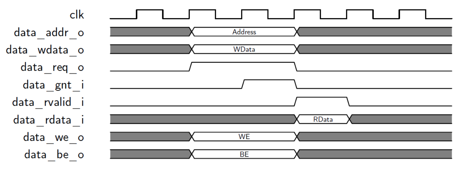
The core has a separate instruction and data bus with the only difference is that the data bus has write functionality. The protocol is very simple. The bus has the standard clock, address, the incoming read data and the outgoing write data. The core starts a transaction by setting the appropriate values in the bus and issues a request. The peripheral responds with a grant signal when it has accepted the values. When the grant signal is set, the core can change the signals for the next transaction. When the peripheral has finished processing the transaction and if it’s a read operation has the set output in the bus, it issues the data valid flag.
 PULPino data bus transaction (image taken by the PULPino user manual)
Coremem
The coremem module is used to for handing all interactions with the bus core. Since PULPino has 2 buses, the module is used twice, one for the ROM and one for the RAM and peripherals. The coremem essentially generates the CE and the WE signal if it is a write operation, when there is a request from the core and waits for only cycle until it sets the grant and valid signal.
The coremem design assumes that all peripherals are able to write the data into one cycle. If a new peripheral needs more cycles to finish the operation, the coremem should be modified, to introduce the extra cycles.
Bus
The minion SoC uses a custom tight coupled bus for communication of the core with the peripherals and the memories. For the core’s instruction bus, the ROM is directly connected with the coremem_i module that handles the protocol handshakes.
The bus addresses are taken from the core’s 4 MSBs data bus addresses in one hot configuration, creating 16 distinct memory regions. Each of the 16 memory regions are mapped to each peripheral and memories.
The peripherals and memories are using the one_hot_rdata[15:0] array that each position is related with the equivalent address, to store the preselected information. That way the peripheral’s SFRs are created. The read operation and bus address creation happens in a always_comb block. The 16 loops that happens in the for loop corresponds to the 16 bus addresses. The address is created when the core_lsu_addr[23:20] is equal to the address number. Finally the correct read data is stored in the core_lsu_rdata, selecting the one_hot_data_addr array element that is equal to the bus address.
Writing operations are triggered when the we_d signal is set, along with the corresponding one_hot_data_addr. The peripheral write operations happens in the following always block that is triggered in a reset or a positive cycle edge. If a reset is set, the SFRs take a default value.
| Type | Memory region | Bus address |
| ROM | 0x000000 | 0 |
| RAM | 0x100000 | 1 |
| UART | 0x200000 | 2 |
| SD | 0x400000 | 4 |
| GPIO (LED, DIP) | 0x700000 | 7 |
| PS2 | 0x900000 | 9 |
| VGA | 0xA00000 | 10 |
In order to modify the bus and add more memory regions, the user should change the width of the one_hot_data_addr keeping it equal with the one_hot_rdata, adding more MSBs of core_lsu_addr to the one_hot_data_addr address generation, modify the for loop generation and . all changes should happen in multiples of 2. Since the RAM and ROM locations are hardwired to the C linker scripts, extra care should be taken that the RAM & ROM hold the same memory region. Off course any modification in the memory locations should be reflected in the software and the SFRs addresses.
memories
The SoC uses one RAM memory to hold variables and a ROM to hold the program running. The implementation lies in the code.v & data.v and it’s generated by the compiled program, using the romgen software. The implementation is based on Xilinx block ram specific modules.
Peripherals
The minion SoC has the following peripherals integrated:
-
UART.
-
PS2.
-
SD card controller.
-
VGA.
-
GPIO (LED, DIP switches).
All the peripherals are used from the rocket core. In my project there wasn’t a need to use the peripherals besides the UART and LEDs.
The GPIO operation is pretty straightforward. There is a SFR that you can write the LED values and there is a SFR that reads the DIP values.
There are 3 SFRs for the UART.
-
a status SFR that has information about the state of the UART, plus the value of an incoming byte.
-
A SFR that holds the value for baud rate generation.
-
The Tx byte SFR.
A Tx operation happens when the Tx value is send to Tx SFR and if the UART is not currently transmitting. For a Rx operation, the UART has a FIFO connected to the Rx line. The read operation is triggered by making a write operation in the status SFR. When that happens the FIFO stores the value in the 8 LSBs of the status SFR.
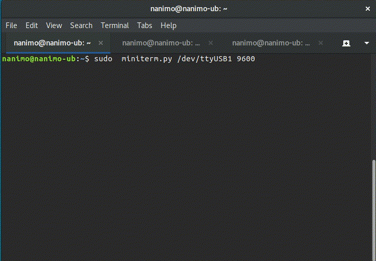
The baud rate calculation uses the following equation: SFR value = clock frequency/ (baud rate * 4). For the arty project that has 25MHz frequency and a 9600 baud rate, the equation is modified to 25.000.000 / (9600 * 4) = 651.
Modifications
During the designing phase of the CLS configuration, I identified some improvements that could be made to minion SoC.
Coremem
While examining the coremem module, I saw that the code had unreached states (WRITE_DATA, WRITE_ADDR) because of constant assignment of aw_ready_i, ar_ready_i and w_ready_i signals. The states could further reduced from READ_WAIT, WRITE_WAIT to WAIT but I left it that way because I think code is more readable. Removing the unnecessary code simplified the module, which was then now reduced to a simple one cycle delay.
Moreover it was found in multiple places in the minion_soc, that the core_lsu_req&core_lsu_we signals were used to access a peripheral in the case of a data bus write. That functionality was identical with the use of the coremem_d’s signal we_d. So all the signals were replaces from the we_d signal. That modification gives a clearer code, with the write of peripherals trigged only from one place.
UART status
The UART status SFR (memory location 0x300.000) has a lot of information about the state of the UART. This included the uart_wrcount variable that shows the number of the incoming bytes stored in FIFO. IMO the number of available bytes in the FIFO is much more critical information. The uart_rdcount shows the number of bytes that are read from the software. I replaced the uart_wrcount with the uart_rdata_avail that holds the available bytes in the FIFO. The information is taken by subtracting the uart_wrcount and uart_rdcount.
Peripheral modularisation.
The SoC uses a custom tight coupled bus for the connection not based on AXI. In the minion_soc.sv there is the bus implementation and the connection of the core, with the RAM,ROM and the peripherals used. This makes the code less clear and more difficult add new peripherals. I made an attempt to separate the bus logic and the peripherals from the minion SoC, so the code is more clear and for me to better understand the bus logic. This attempt provided useful information that was eventually used in the code generation. IMO this approach lead to more clear & concise code.
The peripheral bus has the bus address, bus_write and bus_read array, which have the same functionality as the original bus signals. The extra bus_we & bus_ce arrays, are added. The variables are used to signal a read or write operation in the bus. Each peripheral must access the corresponding bus_we & bus_ce by selecting the correct array member. The peripherals are then responsible to read or write the correct SFR based on the bus address.
The memconfig module (the naming could had been better) has all the bus functionality and is responsible for the core and peripheral interaction. The module generates the bus_we and bus_ce signals. The module also integrates the coremem_d, the module that handles the core’s data bus operations. The signals are generated in the similar way as the data read signals in the core’s data bus.
Note that this code was left unfinished so it is possible that it contains bugs. In the future that work could be merged with the code generation in the form of templates.
Software
This section describes the software developed for running in the minion SoC.
minimal assembly
For the first experimentations with the platform, I created an assembly program. The reasons behind using assembly: a) Learning assembly, gives you a better understanding of the architecture. b) For easy programs, such as the one I created, the manual written assembly code is significant less complex than the equivalent produced from a compiler. c) The lack of a JTAG module lead to most of the debugging happen through the studying of waveforms and hex values. Being familiar with the assembly program and the assembly structure made debugging a lot easier. d) It was a lot easier to setup the environment for the assembler than the compiler.
The first experiment was to see the inner workings of the SoC and if everything was ok. For that reason a very simple program was loaded in the simulator. The program binary was loaded by hand, using the initial function of verilog, in the mem_tb module. The program did a continuous increment on the values of the x1 register. Using the signals generated from the simulation, I was able to verify to correct operation by looking into the instruction and data bus signals.
  _start:
    nop
    addi x1, x1, 1
    nop
    nop
    j _start
Finally I wanted to see if my understanding of the core and peripherals connection was correct. For that reason I made a simple program that transmits a “Hello minion” message through the UART and then blinks the LEDs. The program it’s very simple, it first loads SFR and RAM variables memory addresses into registers. Those registers will be used later to access the contents of the SFR’s through indirect memory addressing. The _print_str_ loop transmits the message, the _loop blinks the LEDs and after that the delay loops for ~100ms. You can find the code here.
One of the most confusing issues that I had to face was to get used to how the memory locations were calculated in progmem. The instruction bus address to progmem leaves the 2 LSB bits core_instr_addr[15:2]. So any memory inside the progmem would had to be stored in a address shifted by 2 in order to correspond to the address request from the core e.g. The core’s boot address is 0x80 memory location, the instruction hex value had to be stored in the 0x20 memory location inside the progmem.
Minimal C
In V0.4 of the minion subsystem there isn’t a C program for the users to base and build their own program. In my case I needed a minimal C program to use it in testing and verification for the changes that I made in the minion SoC, both in simulation and in the actual hardware. For that reasons I created a minimal C program. Also the program was designed with the intention to be easily understood and used from beginners. The bootstrap and hello software couldn’t be used for that purpose because a) bootstrap has a lot of functionality used from the rocket core b) the hello example doesn’t produce the code & data verilog files that are needed to run the software in the minion SoC. Also the project contains a lot of files that are not necessary used from the program and that could be confusing to a beginner.
The program blinks the Arty LEDs, outputs the “hello minion” string in the UART after the reset, echoes a received character in the UART and sends a message if a button is pressed through the UART.. In the verilator simulation, the an UART test bed was used and the minion SoC module was modified so that it would output the actions in the simulation terminal.
The necessary files to compile, link and use the software in the minion SoC were copied from the hello software. The bootstrap makefile was used as a template for the project and modified for use with the minimal C files.
The minimal.c of the minimal program is very simple. It calls functions defined in the minion library. The minion library is a very primitive HAL for the minion SoC. The functions for the LED and the UART operation, were taken from the minion_lib library, found in the hello program. The functions were slight modified by adding a preprocessor definition for the peripheral’s SFRs addresses, so the code is more clear to the user. The functions are pretty shelf explanatory: The to_led() outputs the data value to the LEDS and the from_dip returns the switches value. The blocking functions uart_recv() and uart_send() receives/sends a byte to the UART. The uart_send_buf outputs the contents of a buffer. The uart_bytes_available() returns the available bytes in the Rx FIFO, this function is used in conjunction with the uart_recv only when there is available bytes in the Rx FIFO so it won’t block the main routine waiting for an incoming byte. The uart_init() calls the uart_set_baud which sets the UART baud rate to 9600. In this version the value 651 for setting the baud rate is calculated by hand. Finally the uart_tx_status returns the Tx status of UART. A delay function was added with a approximately delay of 200ms. The delay is used from the example in order to make the change in the LEDs visible to the human eye. The utilities.c holds empty functions, needed from the linker script.
A future expansion of the example could use the rest of the available peripherals in the minion SoC.
Minimal C CLS version
The minimal C CLS version has the same functionality with the minimal C but with a few modifications for the CLS configuration. The i variable is used for keeping the LED value even after a CLS triggered reset. During a reset all variables are initialized to zero. This operation is overridden by defining the i variable as a pointer and selecting the memory address by hand. The chosen memory location must be far away from the rest of the variables so it’s not overridden by accident. In a normal reset the variable should be initialized to 0. The reset_source function returns if the reset triggered from a CLS fault or from the general reset so it would initialize the variable. This solution is a bit hacky and in the future the linker script should be modified in order to incorporate this functionality.
Ports
The minion subsystem in minion-v0.4 version didn’t supported the Arty FPGA board or any support for a simulator. In order to run the code I needed to port them myself.
Verilator
There were 2 main options for a simulator, the integrated simulator in the Vivado suite and the verilator. While the Vivado simulator would have been the easier choice to use, the Vivado suite itshelf requires many CPU resources that made the use in a virtual machine difficult. The other reasons that verilator was used was that the Rocket core simulation is in verilator. The use of verilator could enable a future integration of the minion SoC in the rocket core simulation. in V0.4 of the lowRISC, the minion SoC behaviour in the simulation is emulated by test bed files. Also verilator uses C++ that I’m familiar with.
The rocket core verilator project was used as a template for porting into the minion SoC. The Makefile was modified in order to select the verilog files used from the minion SoC. Most of the work was to identify which files were actually used in the pulpino core.
The minion SoC uses some modules that are Xilinx specific. The FIFO18E1.v file had the simulation implementation of the FIFO modules used. The file was taken from the Vivado installation. The progmem and datamem modules were using Xilinx modules that I couldn’t locate. The modules functionality were identical, also they were simply enough to recreate in a testbed module. Moreover using the verilogs $readmemh() function I was able to easily load the minimal C example running in the minion core. For the rest of the modules, dummy testbed modules was added in the xilinx_tb.v.
Again the rocket core simulation module was used as a template for the veri_top.cc. The original file was stripped away so it would have the minimal needed functionality for the minion SoC. Also the top signals were modified so it would reflect the signals used in the minion SoC. The global library files were directly copied into the project.
Running make in the vsim folder triggers the verilator program compilation. If everything is ok, the required files are stored into the obj_dir folder.
The run_sim script is used to start a simulation. Every signal is saved in a vcd file during the simulation. After the simulation is finished, the minion SoC’s behaviour could be studied by viewing the generated waveforms, running the “gtkwave obj_dir/verilated.vcd” command. Moreover the verilog $display() function was used to display debug messages during the simulation.
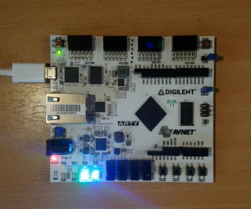
Arty
The nexus4ddr project was used as a template for the arty port. A new vivado project was created for the Arty port of the minion SoC. During The board files needed for vivado to support Arty, were imported by following the digilents guide found here. Again as in the verilator port, the most difficult task was to find which files were actually used from the minion SoC. That process was found through trial and error.
The Xilinx clock IP (clk_wiz_arty_0) was added in the design, the wizard creates the clocks needed for the minion SoC, based on the parameters taken from the nexus4ddr. The pin_plan_arty constraint file was taken from Digilent’s github and modified so that it has all the information needed to map the I/O pins of the FPGA to the minion SoC design. Finally The top_arty.sv file connects the minion SoC with the clocking wizard and only the I/O pins used from the arty, Using the top arty file enables to have different configurations for each board ports, without needing to modify the minion_soc file, thus keeping it identical for all boards.
The arty and the nexus have different resources available, so the mapping is slight different. The 8 LEDs of the nexys were mapped to the RGB LEDs of the arty and not in the 4 LEDs. The reset is mapped to the reset button of the arty. The UART Rx & Tx was mapped to the onboard ftdi USB to serial converter. The arty doesn’t include onboard a SD card, VGA and PS2 peripheral so the pins are not mapped in the arty port. Digilent offers that peripherals in the form of PMOD extension boards, that can be used with the arty. In the future the port could be easily expanded to include the rest of the peripherals with the PMODS . The only reason that the PMODS weren’t included in the design from the beginning was that board wouldn’t arrived on time for me to use them.
The project uses the code.v & data.v files from the minimal C example. The files are not included in the repository so the user would have to either compile the project or his own project.
The SD peripherals clock wizard (clk_wiz_1 sd_clk_div) is not included in the repository as the clock wizards of the boards, so the user would have to either add it himself or if the SD peripheral is not used, remove the IP’s code in the minion SoC and directly assign the minion SoC clock to the SD clock “ assign msoc_clock = sd_clk_o”. A slight more difficult solution, if the user doesn’t want to use the SD peripheral, is to remove all SD functionality in the minion SoC.
| Component name | clk_wiz_1 |
| Input clock frequency | 25 MHz |
| Output clock frequency | 5MHz |
| Output clock clk_out1 name | clk_sdclk |
| Dynamic reconfig | enabled |
| Dynamic reconfig interface options | DRP |
Core Lock Step
In core lock step we use redundant CPU cores, running with the same inputs and comparing each core output. In case there is an SEU during operation, it’s effect would be shown in the affected core’s output.
Issues
The CLS configuration offers protection from SEU’s by continuously comparing the output of each CPU based on common inputs. An SEU could effect a part in the CPU that doesn’t have immediate effect in the output and could manifest later.
-
The design of the CPU.
-
PULPino Performance counters.
-
Operations that store values on PULPino registers.
The LowRISC minion subsystem is still under development and the CPU core could change in the future, for that reasons the design of the CPU would not be investigated.
Since operations that store the result on the CPU registers don’t generate an immediate output. A solution could be that the registers are exposed and compared by the CLS unit. Another solution would be to protect the registers by using techniques like TMR and ECC. Both of that solutions would require modifying the CPU which is not wanted as stated above.
Since operations on registers are often and in C when a function is used, it loads/stores the registers, an SEU effect would be seen in relative few cycles.
Assumptions
-
The CLS configuration is focused only in the protection from SEU’s and from permanent faults.
-
The protection of the peripherals, memories and the CLS assist unit itself won’t be examined during this phase.
-
The debug unit is not used during the CLS configuration.
Fault detection behaviour
The first and easiest fault handling is that the CLS unit resets the CPU cores. Since it doesn’t reset the RAM or other peripherals, the program could be written in a way that assumes operation as quickly as possible.
Another solution could be that the CLS unit generates an exception, either by modifying the CPU core in order to add the exception or by assigning an interrupt. The interrupt approach better because is simpler and doesn’t need any CPU modification.
Finally checkpoints could be used to restore the faulty CPU in the last know healthy state. The checkpoints could be either introduced automatically or manual from the developer. The checkpoint functionality should be achieved with the support of software and hardware:
-
Hardware: Adding the mechanism in the CLS unit that stores the state in the form of the instruction address. This could be done with: a) extending the instruction set including the checkpoint instruction or b) having a memory addressable register that stores that state with ordinary store instructions.
-
Software: Since it’s not easy to store the exact state of the CPU (registers) the program execution should be altered so when a checkpoint is used, it is ensured that no previous values in registers are used.
One of the advantages of triple core lock step is that by having 3 cores using voting, the core that generated the issue could be found. Using a restore mechanism like checkpoints or exceptions, the faulty core could be re synched in a few cycles, thus removing the need to restart the program.
Implementation
The core lock step implementation was pretty straightforward after a better understanding of the minion SoC and the pulpino core was achieved.
The CLS configuration was placed in the minion_cls.sv module. The module has identical I/O with the pulpino core and is meant to replace the pulpino core in the minion_soc.sv. The only modification required in order to use the CLS configuration is by adding the _cls extension in the riscv_core of the minion_soc.sv. That way minimal modification of the minion_soc is ensured. The module has 3 pulpino core instances, the cls_cmp_unit that compares the core’s output and signals a fault and the cls_handler_unit that implements the fault recovery.
The cores are configured in 1 master and 2 slaves. The inputs are connected directly from the module top. The 3 core’s output are connected to the cls compare unit but only the master core is connected to the module’s output ports. Extra wires are only required by the slave cores and the naming is differentiated from the cls1 and cls2 extension. The only reason that the cores are separated into 1 master and 2 slaves is by connecting the master’s outputs directly to the modules output port and not by another module, it leads to less and more clear code.
The cls_cmp_unit compares the outputs of all cores and issues a fault when is detected. The implementation was straightforward, the only difficulty was in the code design in the comparison of that many signals. The comparison starts only when the any core issues a request signal for the instruction or data bus. If there is a request in the instruction bus the unit then checks for the addresses. For the data address there is an extra check in the write data when a write is performed. It should be noted that the comparison unit doesn’t check for inconsistencies in the signals when a request is not issued. For more concise code the data and instruction request signals from all the cores were concatenated into a single signal respectively. A single fault signal is used but if the recovery strategy requires it, the fault signal could be extended in order to show what triggered the error.
The cls_handler_unit handles any faults detected from the compare unit. Since the recovery strategy is to reset all cores, the unit intercepts the reset signal from the top module to the cores. The unit has 2 tasks: a) to monitor the top module’s reset signal and forward a reset to the cores when issued from the top module. b) Issue a reset to the cores for 1 clock cycle when a fault is detected. The functionality of the module could have been placed in the comparison unit but in my opinion the separation lead to a better design.
Besides the minion_cls, the coremem module was modified in order to ensure fault containment. In the case that a fault happens during a data write operation, there is a chance that the erroneous operation happens before the handler unit issues a reset. For that reason the coremem module is modified in order to introduce one extra cycle delay during write operations. The module delays setting the ce, we signals to the peripherals and the data grant signal to the cores.
A reset source SFR was added, the SFR has 0 if the reset was triggered from a normal reset and 1 if the reset was triggered by a CLS fault. That way the software knows the reset source.
fault injection
Faults were simulated by injecting errors in the CLS design. These tests were the only way to ensure that the design was working. The errors are created by modifying the values in variables during runtime usually by introducing multiplexers. To my knowledge there isn’t a framework that could make automated integration of the multiplexers in the CLS design, so the integration would had to be made manually. Introducing fault injection in random places in the pulpino core would have been a difficult and cumbersome task so it was avoided. A more plausible way was to inject errors in the cores output.
The fault_injection_assist module was introduced in the minion_cls.sv. The module overrides the cores outputs and when a fault injection was issued it toggled the selected signal. The new signals are defined in the minion_cls module. In order to use the fault injection, a “_finj” should be added in the signal name, going to the cls comparison module. The modules internal implementation uses the fault_injection_mux module which is a simple multiplexer. In normal operation, the multiplexer forwarded the incoming signal value to the output. If a fault injection was requested and the index matched the multiplexer, it toggled the incoming signal’s value. The first implementations tried to modify the existing signals kby XORing to itself but that created an infinite feedback loop.
One key issue was finding the best approach for the fault injection timing. Without a model of the SEU generation in space, the best way was to inject faults pseudo randomly in a time range that would make sense. The first attempt was to use a hardware pseudo random generator but it was quickly abandoned for a more swift solution, implemented in software. In the beginning all the output signals were exposed to a fault injection but in order to make testing simplier and reduce the used FPGA resources, only the data and instruction bus request and address signals were used.
The first tests were made in verilator. The verilog top module was modified in order to expose the fault generation and signal index to the verilator C++ program. In verilator test program a simple menu was created, where the user selected from the terminal if there would be a fault injection and in what signal. The menu was triggered by C++ pseudo random generator. As it was noted above in the first implementations of the fault injection unit a XOR was used in the affected signals. When the implementation was tested in the verilator, a non convergence error was triggered, that lead to the discovery of the bad design. Due to the added resources, the running simulation took longer to evaluate, so the delay running in the main loop of the minion hardware was reduced.
After the successful testing in the simulator, the design was tested in the actual hardware. A Xilinx VIO debug IP was used to trigger and verify the fault injection. The VIO IP connects the Arty board through JTAG to the Vivado suite in real time. There the VIO inputs were used to monitor critical signals in order to verify the correct behaviour of the CLS configuration. A VIO output was connected to the fault injection unit, there a button in Vivado was used to trigger a fault. The minion SoC with fault injection unit along with the VIO IP required more LUTs that there were available in the Arty FPGA, I had to removed the SD peripheral in order to free resources. Also the fault injection unit was modified to allow only one signal to be used, in order to limit resources usage.
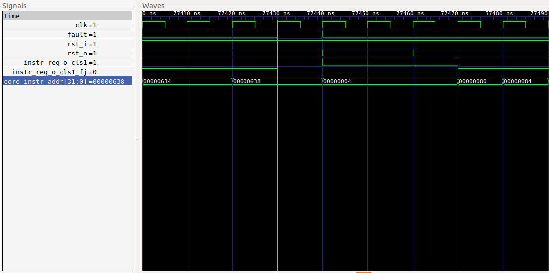 Fault injection in simulation. The fault is injected in the red cursor.
Packetcraft
In order to assess the CLS configuration, a test application was developed. The application implements the test service, a subset of the command and data handling protocol, running on UPSat. The test service is the equivalent ping of the computer networks. The user sends a test service telecommand and the subsystem, which in our case is the Arty, responds with a telecommand. For more information about the protocol see the ECSS-E70-41A specification.
The packet.py sends continuously a test packet and counts the responses from the Arty, while it randomly triggers a fault injection. If there is a difference between the number of packets sent and received, it would mean that something went wrong due to the fault injection. The fault injection is triggered by an Arduino connected to the fault injection pin in the Arty.
The minion SoC runs with a CLS and fault injection configuration. The test_packet.c found in software/packetcraft implements the test app in the minion SoC side. The software is a very simple implementation, it reads the incoming characters, has a small delay of ~5us that simulates the packet processing time, check if there is a valid packet and responds. The original software does multiple checks which there wasn’t necessary to implement.
For the test I started to find which Tx period (packets send from packet.py), is the limit that the SoC starts losing packets without fault injection. The SoC had 20% packet losses in the a Tx period of 0.08 which is very good as the application is not optimized and the tx packet takes 0.01 sec to transmit. After that I started to find the fault injection interval that the SoC starts losing packets. At average of one fault injection per 0.025 sec, the SoC had 1.2% packet losses, at 0.01 sec there was 39.6, while at 0.005 there was 100% packet loss. This is very promising results since the expected rate of faults induced by radiation is farr less than that.
| Tx period (Sec) | Fault injection average period (Sec) | Packet losses (%) |
| 0.08 | 0 | 20 |
| 0.05 | 0 | 50 |
| 0.1 | 1 | 0 |
| 0.1 | 0.5 | 0 |
| 0.1 | 0.05 | 0 |
| 0.1 | 0.025 | 1.2 |
| 0.1 | 0.01 | 39.6 |
| 0.1 | 0.005 | 100 |
Code generation
The minion SoC functionality is implemented in the minion_soc.sv. In that file the PULPino core along with the memories and peripherals are placed together. In order to make a minion with a different configuration the user would have to have modify the file, a cumbersome action that would be intimidating for beginners and users that don’t have a good understanding of the SoC.
For that reason I made a generator that takes a JSON configuration file and produces the minion SoC. The project is still a work in progress and not a full working project. Using the generator in the future enables users to easily use the Core Lock Step configuration without writing code.
The generator is based on python and jinja2 for the templating engine. Other options that were consider was the use of Chisel, myHDL and pyHDL but a simpler solution in terms of dependencies and ease to use, was preferred. One design intention was the minimal verilog code modification for the template.
The JSON configuration file holds the configuration parameters of each module. The usual options are the peripheral’s name, the memory region that it uses and if the module could be used multiple times the module’s number. Each module could have it’s own specific parameters.
The CLS configuration in core is enabled by setting the core_lockstep parameter to true. In the case fault injection is needed, the fault_injection must be set to true. The fault injection trigger is set by selecting either a pin, a button or a VIO IP module.
The templates were derived from the minion_soc.sv. Each template could have:
-
a port template that defines the module’s I/O ports, if the module has I/O ports.
-
an instance template that defines the peripheral, along with any variable that is needed. This template usually has the read SFRs and the memory region that it uses. Finally if the peripheral could be used multiple times e.g. UART, all the names of variables and modules uses a peripheral_number template variable in order to distinguish itself from each different peripheral instance.
-
an init template that has any register that needs to have a specific value at reset.
-
a bus template that has holds all the write SFRs.
Any custom peripheral could be added by implementing any of the above templates.
The following templates are available:
-
the core template has the CPU core.
-
the LED template.
-
the DIP switches template.
-
UART template.
-
PS2 template used for connection with a keyboard.
-
SD controller template.
-
VGA template
The generator creates the minion_soc.sv, coremem.sv, top_arty.sv and the minion_cls.sv if CLS is used. All generation is based on their corresponding templates.
The peripherals use memory mapped SFRs to exchange information with the core. The memory location of each SFR is used in the HAL from the software running in the SoC. One of the key aspects of the code generation is the ability to quickly modify each peripherals SFR memory region without requiring to rewrite the HAL by generating the file that holds the memory locations.
Note that this code is still under development so it is possible that it contains bugs. Currently the more than 1 UARTs implementation doesn’t work.
CLS power and size differences
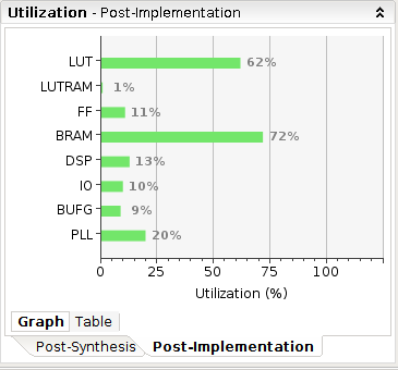
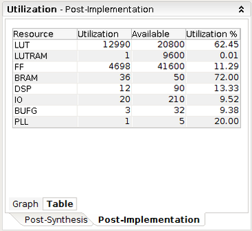
One of the key metrics of any protection techniques, is the changes in resources usage. In this section the resource usage of the CLS configuration and the original SoC are reported. As we can see in the tables, the CLS has 26.47% overhead in LUTs, 3.51% in flip flops, 6.66% in DSP. The other resources remain the same (the BUFG are not taken into account).
The other critical factor for use in cubesats are the power dissipation. The added 8mW is not an issue. Also the general power dissipation makes it usable for 2U cubesat, as In UPSat the onboard computer used 0.198W.
 |
|
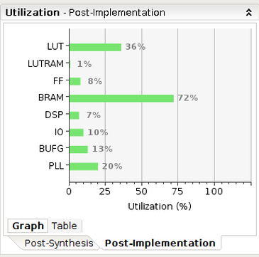
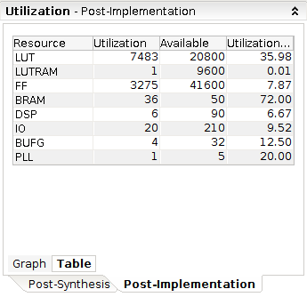
Resource utilization with CLS (top) and without (bottom)
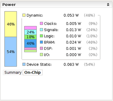
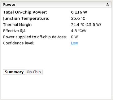
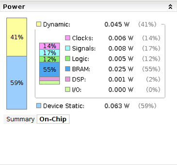
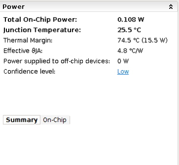
Power usage: with CLS top) and without (bottom)
Thoughts and future work
One of the reasons that I started the GSoC project was get more familiar with HDL and FPGAs while I contributed to an open source project. Even though the CLS configuration is experimental and needs more work to be done, I believe that I made one step towards more open source in Space. Also debugging the minion SoC in the FPGA without JTAG is bad.
After the GSoC I would like to continue working in the code generation project. Using the code generation made design & testing simpler. I wish I started working in the project earlier in the summer.
Finally I would like to thank my mentor, Alex Bradbury for his help and patience, Mr Aris Stathakis that lend me his arty board and Google for making GSoC.